Pre-review
In the last issue, Xiaobian took everyone to see the magic of the shell. With the Gemini300 field emission scanning electron microscope, the fine structure and composition analysis of the shell surface material, as well as the study of cracks at the closing point, suddenly felt that they were also tall. Up, there is wood, this issue, Xiaobian led everyone into the photoelectric materials, and then revealed a little, quantum well materials, together to witness the scanning electron microscopy technology in the quantum well research!
Overview
So what is a quantum well? Xiaobian explains it a little bit. Quantum wells are potential wells of electrons or holes with distinct quantum confinement effects formed by the arrangement of two different semiconductor materials. A quantum well device refers to an optoelectronic device that uses a quantum well material as an active region.
First, the construction of quantum wells
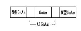
As shown in the figure below, the basic structure of the quantum well device is that two N-type GaAs are attached to both ends, and there is a thin layer in the middle. The structure of this thin layer is composed of a composite form of AlGaAs-GaAs-AlGaAs. When unbiased, the potential energy of each region forms a potential well with the region corresponding to the intermediate GaAs, so it is called a quantum well. The electron's motion path is from the left N-type region (emitter) to the right N-type region (collector), which must enter the quantum well through the AlGaAs layer and then penetrate another layer of AlGaAs. Although quantum well devices are newly developed devices, they have been applied in many fields, such as quantum well infrared detectors, GaA s, InP-based superlattices, quantum well materials, quantum optical communication, and quantum structure LEDs. As production levels increase, it will be more widely used.

Basic structure of quantum well
Second, the microscopic world of quantum wells
Quantum well materials are generally prepared by molecular beam epitaxy (MBE) or metal organic oxide chemical vapor deposition (MOCVD) techniques. For the observation of the interface structure of quantum well materials, such as stacking faults occur during crystal growth. The formation, characteristics and distribution of defects such as dislocations are generally observed by high-resolution transmission scanning electron microscopy (TEM) to determine the relationship between the microstructure parameters of the material and the macroscopic performance parameters of the device. It is well known that the preparation of transmission samples is strict and the preparation of samples is difficult. First, the film surface of the sample is used for bonding, and then the wire is cut to 3 mm × 1 mm. Secondly, the sample is ground and polished to a thickness of about 60 μm and then polished to 20 μm. Finally, the sample was bombarded to 10 nm or less using an ion thinner. This process requires high technology, and each step requires experience. It is not something that most people can do, and the cost is high. Compared with scanning electron microscopy, the sample preparation is simple, and the conductive sample is directly fixed on the sample stage with conductive glue. Observations are made in the chamber. For non-conductive samples, we also have our own solutions. One is equipped with an ion sputtering device, ie, gold is sprayed, and the other is low voltage mode. Low-voltage imaging is the development trend of modern field emission scanning electron microscopy. Low voltage Imaging can present the surface details of the sample, reduce the charge (discharge) of the non-conductive sample, and reduce the damage of the electron beam to the sample.
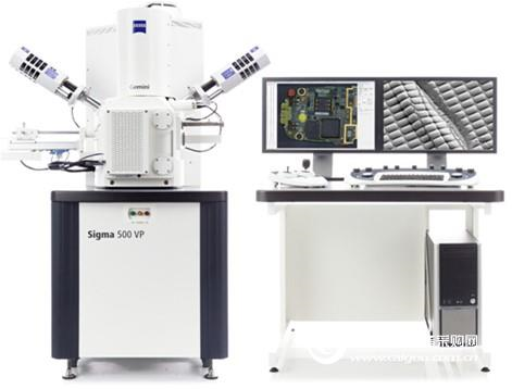
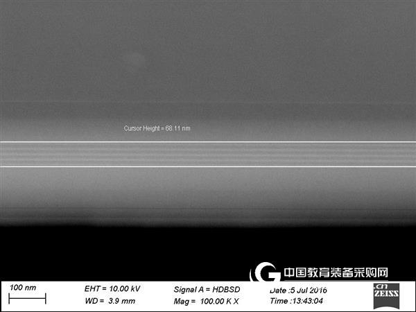
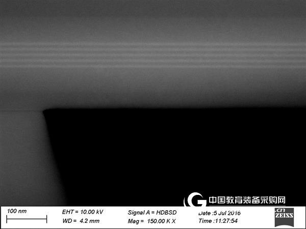
For film materials, the following is the quantum well material measured by Zeiss sigma 500. We obtained backscattered images of the quantum wells at 100,000 and 150,000 times. It can be seen that the sample interface is bright. The contrast bands with different darkness levels have clear boundaries, smooth interfaces, high layer distribution accuracy, good periodicity, and thickness of 68.11 nm. The wells and barriers alternately appear to determine the periodic thickness.


postscript
With the rapid development of molecular beam epitaxy and metal organic chemical vapor deposition technology, people have been able to grow high-quality ultra-thin semiconductor materials with atomic scale and smooth interface, which can precisely control the composition of thin layers in the growth direction. And thickness, in order to achieve superlattice quantum well structure, so the research of lattice quantum well structure materials and applications has rapidly developed into one of the most important frontier topics in semiconductor physics and solid state physics, and scanning electron microscope must be large Show your skills, then follow the pace of small series, we will follow Zeiss scanning electron microscope to witness the glory of the history of photoelectric materials!
What's the highlight of the next issue? Stay tuned!
Charming ombre dark blonde wig and very stylish design with natural pretty looking and soft touch. Two tone long straight wig with bangs, natural and soft like real human hair, wig with bangs makes you more cute, fashion. Perfect for cosplay, party, halloween, concerts, theme parties, dating etc.
Full machine made none lace wig with side parting, adjustable average cap size. There are two adjustment straps inside the wig, which can be intertwined to a fixed position to suit different head sizes.
Our long wavy wigs no chemical and weird smell, only high standard meterial used. It is the best Synthetic Wigs, soft and smoothly
Ombre dark blonde very stylish design with natural pretty looking and soft touch. You can wear it to parties or for daily use.
Fast shipping, stocked in large. If you have any problems about the hair ties and shipping, please contact us freely. We are sure to give you a pleasant shopping experience.
Warm tips: All full machine made synthetic wigs happen to be minimum shedding and tangling which is normal.
Synthetic Wigs,Synthetic Hair,Synthetic Hair For Sale,Synthetic Wigs For Sale
Xuchang Le Yi De Import And Export Trade Co., Ltd. , https://www.lileaderbeauty.com
